
Course 061 IC Reliability, Fault Isolation, and Failure Analysis
Available course dates
This course has no planned course dates.
If you are interested in this course, contact us at cei@cei.se
TECHNOLOGY FOCUS
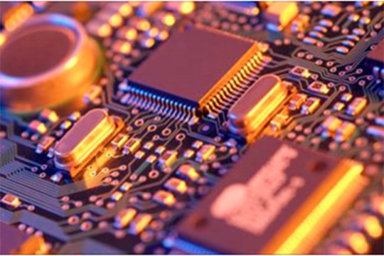
Quickly finding and eliminating defects in electronic devices is critical to all levels of the many businesses including ICs, PCBs, automotive, consumer, and IoT. This can directly affect technology development, manufacturing yield and time to market, reliability, serviceability, and client satisfaction. Many factors contribute to the achievement of high yield and reliability and significantly impact product performance and cost. A thorough understanding of product and technology reliability principles and mechanisms of failure is essential. A fundamental knowledge of defects and failure mechanisms enables the up-front achievement of these technology goals through circuit and layout design, device design, materials choices, process optimization, and thermo-mechanical considerations. Fault isolation, failure analysis, and materials analysis play a major role in the improvement of yield and reliability. Coordination of people in many disciplines is needed in order to achieve high yield and reliability. Each needs to understand the impact of their choices and methods on the final product. Unfortunately, very little formal university training exists in these critical areas of IC reliability, Fault Isolation, and failure analysis.
COURSE CONTENT
This course contans IC Reliability, Fault Isolation and Failure Analysis.
WHO SHOULD ATTEND
This course will be of strong interest to engineers working in R&D, design, manufacturing, and reliability of automotive and consumer electronics, and IoT, as well as management, equipment service, and procurement.
It will be relevant both for companies producing integrated circuits themselves and for those involved as partners in the “fabless/foundry” model.
Daily Schedule
Day 1 – KRISTOF CROES
Definitions and Overview of Failure Mechanisms
- Scaling Trends in IC’s
- Yield, Quality and Reliability
- Lifetime, Failure, Degradation and Failure Criterion
- Failure Time Distributions
- Percentiles
- Accelerated Reliability Tests
- Acceleration Factors and Lifetime Models
- Overview of Failure Mechanism
Front-End-Of-Line Failure Mechanisms
- Time Dependent Dielectric Breakdown of Gate Oxide
- Bias Temperature Instability
- Hot Carrier Injection
Day 2 – KRISTOF CROES
Back-End-Of-Line (BEOL), Far-BEOL and Packaging Failure Mechanisms
- Electromigration
- Stress Induced Voiding or Stress Migration
- Time Dependent Dielectric Breakdown of Intermetal Dielectrics
- Chip Package Interaction
- 3D-related failure mechanisms: Reliability related to Through Silicon Via and stacking challenges
- Packaging-Related Failure Mechanisms
Day 3 AM – KRISTOF CROES
Reliability Methodologiess
- Reliability Evaluation Strategies
- FMEA: Failure Mode and Effect Analysis
- Statistics: Data Fitting Techniques
- Statistics: Techniques to Reduce Uncertainty in Reliability Predictions
Day 3 PM – DAVID VALLETT
IC Fault Isolation and Failure Analysis
- The role of Failure Analysis in Semiconductor Technology Development and Manufacturing
- Differing Failure Analysis strategies for Technology Development, Yield Analysis, and Reliability Engineering
- Client Support and Failure Analysis of Field Returns
- Analytical approaches for Package, Wafer, and Die Level failures
IC Failure Modes and Defects
- Electrical Failure Modes of Logic, SRAM, DRAM, and Analog/Mixed Signal Devices
- Defect Mechanisms in ICs and IC Packages
- Defects in Design, Processing, and Lithography
- Failures Due to Process/Product Interactions
- Test-induced Defects
Fault Isolation
- Electrical vs. Physical Fault Isolation
- Device Characterization
- Prerequisites for Successful Fault Isolation
- Overview of Methods
Electrical Fault Isolation
- Electrical Fault Isolation Purpose, Fundamentals, and Goals
- Time Domain Reflectometry (TDR)
- Electro-optical TeraHertz Pulse Reflectometry (EOTPR)
- SEM and Atomic Force Nanoprobing
- CV Analysis, Pico-current Imaging, Pulsed IV, and Electron Beam Techniques
- Success Factors – Measurement Resolution, Sensitivity, Accuracy, Reliability
Day 4 – DAVID VALLETT
- Physical Fault Isolation Introduction
- Physical Fault Isolation Purpose, Fundamentals, and Goals
- Overview of Thermal, Photonic, Magnetic, and Scanned Particle Beam Methods
- Sample Preparation for Physical Fault Isolation
Photonic Fault Isolation Techniques
- Photon Emission Microscopy (PEM)
- Optical Beam Induced Resistance Change (OBIRCH/XIVA/TIVA)
- Optical Beam Induced Current (OBIC)
- Laser Voltage Probing/Imaging (LVP/LVI)
- Light Assisted Device Alteration (LADA)
- Picosecond Imaging Circuit Analysis (PICA)
Physical Fault Isolation Continued
- Thermal Fault Isolation – Liquid Crystal Analysis, Lock-In Thermography
- Magnetic Current Imaging by SQUID (Superconducting Quantum Interference Device) and GMR (Giant Magneto Resistive) Sensors
- Electron and Ion-Beam Induced Current (EBIC/IBIC)
- Passive Voltage Contrast by Electron and Ion Beam (PVC)
- Atomic Force Microscope Based Physical Fault Isolation
- Success Factors – Measurement Resolution, Sensitivity, Accuracy, Reliability
Device Deprocessing
- Depackaging Techniques – Laser, Chemical, Mechanical, Plasma
- Wafer and Die Deprocessing – Polishing, Chemical Etching, Plasma Etching
- Focused Ion Beam Principles and Applications
Day 5 – DAVID VALLETT
- Physical Imaging
- Optical Microscopy
- Acoustic and X-ray Microscopy/Tomography
- Scanning and Transmitted Electron Microscopy (SEM/TEM)
- Scanned Probe/Atomic Force Microscopy (SPM/AFM)
Materials Analysis
- Basics Materials Analysis Methods for Chemical Composition and Morphology
- Particle Beam Interactions in Solids
- Bulk Composition Analysis: Energy and Wavelength Dispersive Spectroscopy
- Principles of Electron, Ion, and X-ray Techniques: TEM, AES, SIMS, XPS, and TXRF
- Sensitivity and Resolution Comparisons
- Technique Selection Factors
Practical Applications and Future Challenges
- Case-histories and Examples: Time-resolved Photon Emission Movies of Operating Devices; Nanoscale 3D X-ray Tomography Virtual Sections; Defects; Fault Isolation Results, etc.
- Planning for Analysis to Maximize Effectiveness
- Scaling and Material Challenges in Analytical Science
ALL COURSE DATES FOR THE CATEGORY: Semiconductors Technology
035 Introduction to Semiconductor Packaging Technology
036 Silicon Device Technology: Materials and Processing Overview
037 Power Semiconductor Device Technology
075 Heterogeneous integration of chiplets – Defect inspection, metrology and failure analysis
088 Plasma Etching for CMOS Technology and ULSI Applications
099 Integrated Circuit and MEMS Fabrication Technologies
Designed to bridge the gap between device physics and electronic characteristics, the course examines the intricate process flows of CMOS manufacturing and MEMS fabrication, highlighting how these technologies are integrated in real-world applications. A detailed discussion of 3D micromachining techniques further reveals the power of MEMS in creating multifunctional microsystems.
What You’ll Learn
-
The basic physical principles of microelectronic devices
-
Key IC fabrication technologies and how they shape device behavior
-
Silicon bulk and surface micromachining for MEMS fabrication
-
Complete CMOS process flow and technology integration challenges
-
The evolution and ecosystem of modern microfabrication
855 Semiconductor Lithography
856 Alternative Lithography
870 Invention and Innovation – Creation and Management of World Class Patents
Instructor: Dr. Walter F. Lange Dr. Walter Lange, is teaching this two-day class focusing on the fundamentals to enable successful